3D Printing

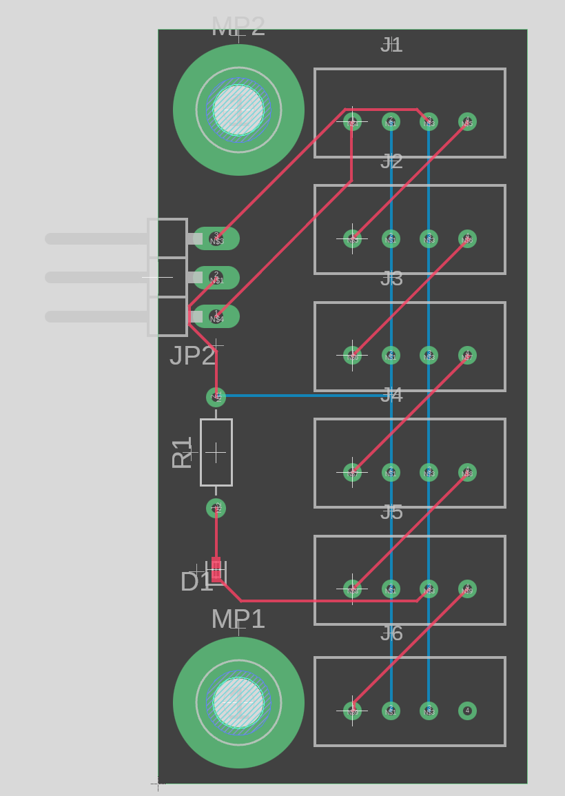
There are several types of 3D printing technologies, also known as additive manufacturing, each with its own unique characteristics and applications. Here are some of the commonly used types of 3D printing:

  • Fused Deposition Modeling (FDM)/Fused Filament Fabrication (FFF): FDM is one of the most popular 3D printing methods. It works by melting and extruding a filament of thermoplastic material through a nozzle, which then solidifies to create the desired object layer by layer. FDM/FFF printers are widely available and commonly used for prototyping, hobbyist projects, and low-cost production.
  • Stereolithography (SLA): SLA utilizes a liquid photopolymer resin that is cured using a UV laser or other light sources. The resin is selectively exposed to light, solidifying the material layer by layer to create the final object. SLA printing is known for its high level of detail and accuracy, making it suitable for applications such as jewelry, dental models, and small-scale production of high-resolution parts.
  • Selective Laser Sintering (SLS): SLS involves the use of a high-powered laser that selectively fuses powdered material, typically polymers or metals, to create 3D objects. The printer spreads a thin layer of powder, and the laser sinters the particles together based on the pattern generated by the 3D model. SLS can produce functional and durable parts and is often used for rapid prototyping and small-batch production.
  • Digital Light Processing (DLP): DLP is similar to SLA, but instead of using a laser, it employs a light source, such as a projector, to selectively cure a liquid resin. The light source projects a complete layer onto the resin, and the exposed areas solidify. DLP printers can offer faster printing speeds compared to SLA and are suitable for applications that require high resolution and smooth surface finishes.
  • Selective Laser Melting (SLM)/Direct Metal Laser Sintering (DMLS): These 3D printing methods are used for metal additive manufacturing. SLM and DMLS use a high-powered laser to melt and fuse metal powders together, creating fully dense metal parts. They are utilized in industries such as aerospace, automotive, and medical, where high-strength, complex metal components are required.
  • Electron Beam Melting (EBM): EBM is another metal additive manufacturing technique that uses an electron beam to melt and fuse metal powders. Similar to SLM/DMLS, EBM is capable of producing strong metal parts and is often employed in aerospace and medical industries for manufacturing critical components.

These are just a few examples of the various 3D printing technologies available. Each method has its own advantages, limitations, and applications, and the choice of technology depends on factors such as the desired materials, level of detail, speed, and cost considerations.

PCB-Routing

PCB Routing is one of the most important processes of creating PCB's. Electrical engineers design the function of the electronic devise but don't actually create placement for the finished product. Product designers and electrical engineers work close together to fit the boards into smaller spaces, improving use case and minimizing footprint of product. We interpret electrical diagrams to PCB layout at a reasonable price, compared to large scale product development. 

Featured

PCB Enclosure

A PCB (Printed Circuit Board) enclosure is useful, several reasons why:

  • Protection: The enclosure provides physical protection for the PCB and its components. It helps safeguard the board from dust, moisture, mechanical shocks, and other potential hazards. This protection is crucial, especially in industrial or outdoor environments where the PCB may be exposed to harsh conditions.

  • Electrical Safety: The enclosure can offer electrical insulation, preventing accidental contact with live components or exposed circuitry. It helps prevent short circuits, electric shocks, or damage to the PCB due to environmental factors.

  • EMI Shielding: Some PCB enclosures are designed with EMI (Electromagnetic Interference) shielding materials. These materials block or absorb electromagnetic radiation emitted by the PCB and prevent interference with other nearby electronic devices. EMI shielding is particularly important in sensitive applications such as medical devices or communication systems.

  • Compliance with Standards: Enclosures help PCBs meet specific compliance and regulatory standards. Depending on the application, certain certifications or regulations may require PCBs to be enclosed for safety, electromagnetic compatibility, or environmental protection reasons.

  • Aesthetics and Ergonomics: An enclosure provides a neat and professional appearance to the PCB assembly. It also facilitates the integration of the PCB into a larger system or product. Enclosures can be designed with features like mounting holes, connectors, and labels for easy installation, maintenance, and user interface.

  • Customization and Branding: Enclosures can be customized to meet specific design requirements or reflect a company's branding. They can be tailored in terms of size, shape, color, and labeling, aligning the PCB with the overall product design or corporate identity.

Overall, a PCB enclosure offers protection, safety, compliance, and customization benefits. It ensures the reliability and longevity of the PCB assembly while enhancing its functionality, aesthetics, and integration within a larger system or product. Note: We do help with design layout using Eagle to implement design with enclosures, if this something you need, please feel free to contact us, we will work closely to help you get your PCB done the way you need it. 

Contact